龚翔薇透射电镜与扫描电镜的区别是什么呢英语
- tem电镜样品
- 2024-06-16 17:57:12
- 348
纳瑞科技(北京)有限公司(Ion Beam Technology Co.,Ltd.)成立于2006年,是由在聚焦离子束(扫描离子显微镜)应用技术领域有着多年经验的技术骨干创立而成。
Transmission Electron Microscopy and Scanning Electron Microscopy: Differences and Similarities

Transmission electron microscopy (TEM) and scanning electron microscopy (SEM) are two widely used microscopy techniques that have made significant contributions to the field of materials science and technology. Both TEM and SEM are based on the principles of electroscopy, where a high-energy electron beam is used to analyze the structure and composition of materials. In this article, we will discuss the differences between TEM and SEM, as well as their similarities.
Appearance and Functionality
The first and most obvious difference between TEM and SEM is their appearance and functionality. TEM is an electron microscope that uses a beam of electrons to form an image of a material's atomic structure. The beam of electrons is directed onto the sample, and the resulting image is captured by a camera. SEM, on the other hand, is a microscope that uses a beam of electrons to scan the surface of a material. The beam of electrons is directed onto the sample, and the resulting image is captured by a camera or other sensor.
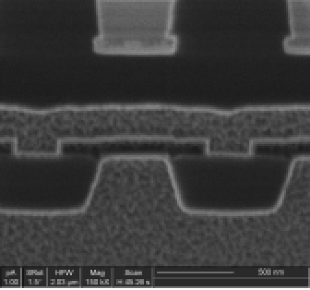
Another key difference between TEM and SEM is their functionality. TEM is primarily used to study the structure and composition of materials at the atomic level. It is ideal for analyzing metals, semiconductors, and other materials that are relatively thick. SEM, on the other hand, is more suitable for studying thin films and surfaces of materials. It is ideal for analyzing materials such as metals, semiconductors, and insulators.
In summary, TEM and SEM differ in terms of their functionality and the type of samples they are suitable for. TEM is more suitable for studying the atomic structure of materials, while SEM is more suitable for studying thin films and surfaces of materials.
Advantages and Disadvantages
Despite their differences, TEM and SEM have several advantages and disadvantages.
Advantages
1. TEM provides high-resolution images of the atomic structure of materials, which are useful for studying the properties of materials at the atomic level.
2. TEM is ideal for analyzing materials that are relatively thick, such as metals and semiconductors.
3. TEM can be used to perform various experiments, such as diffraction, electron diffraction, and spectroscopy.
4. TEM is a relatively slow and expensive technique.
1. SEM provides high-resolution images of the surface of materials, which are useful for studying the properties of materials at the nanoscale.
2. SEM is ideal for analyzing thin films and surfaces of materials, such as metals, semiconductors, and insulators.
3. SEM can be used to perform various experiments, such as electron spectroscopy and chemical analysis.
4. SEM is a relatively fast and less expensive technique than TEM.
Disadvantages
1. TEM requires a high-energy beam of electrons, which can be generated only in a few sources, such as synchrotron radiation or a linear accelerator.
2. TEM is a relatively slow and expensive technique, and it can be time-consuming to prepare a sample for analysis.
3. TEM is not suitable for studying thin films and surfaces of materials.
4. SEM can be affected by surface charging, which can lead to image distortion or loss.
Similarities
Despite their differences, TEM and SEM share several similarities. Both TEM and SEM use a beam of electrons to analyze the structure and composition of materials. Both TEM and SEM can be used to perform various experiments, such as diffraction, electron diffraction, and spectroscopy.
Conclusion
In conclusion, TEM and SEM are two widely used microscopy techniques that have different functionalities and are suitable for different types of samples. TEM is more suitable for studying the atomic structure of materials, while SEM is more suitable for studying thin films and surfaces of materials. Both TEM and SEM share several similarities, including the use of a beam of electrons and the ability to perform various experiments. However, they also differ in terms of their functionality, sample suitability, and cost. Therefore, it is important to choose the appropriate technique based on the specific research question and available resources.
专业提供fib微纳加工、二开、维修、全国可上门提供测试服务,成功率高!
龚翔薇透射电镜与扫描电镜的区别是什么呢英语 由纳瑞科技tem电镜样品栏目发布,感谢您对纳瑞科技的认可,以及对我们原创作品以及文章的青睐,非常欢迎各位朋友分享到个人网站或者朋友圈,但转载请说明文章出处“透射电镜与扫描电镜的区别是什么呢英语 ”